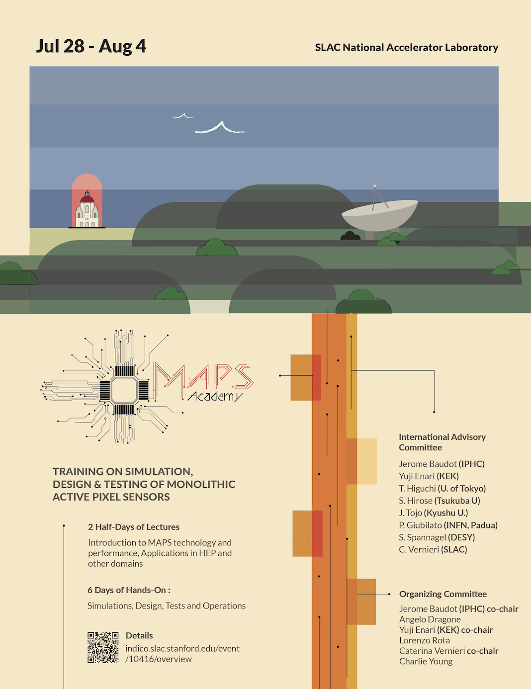
Following the success of the First MAPS Academy held at KEK in Summer 2025, we are looking forward to host the second edition at SLAC , July 28- August 4, 2026.
Overview of MAPS Academy
MAPS (Monolithic Active Pixel Sensor) is a semiconductor detector that utilizes CMOS technology, allowing for miniaturization and a significant improvement in signal processing capabilities. It is also well-suited for mass production, making it possible to create high-performance detectors at a low cost. In future collider experiments, MAPS can be applied to a wide range of uses, from tracking detectors and calorimeter readout to large-area muon detectors.
Designing and developing such systems requires a substantial amount of fundamental knowledge and expertise. The MAPS Academy aims to provide a program that serves as a stepping stone for acquiring these skills. The MAPS Academy is a school for young researchers, such as senior graduate students (Master to PhD students), postdocs, or young faculty staffs, who wish to acquire a deeper knowledge of the development of the MAPS technologies.
Participation in the MAPS Academy requires an application. Selected young researchers through a pre-screening process are invited to the MAPS Academy including lectures and hands-on sessions.
We welcome applications from outstanding young researchers in particle or nuclear physics and related fields, as well as sensor engineering.
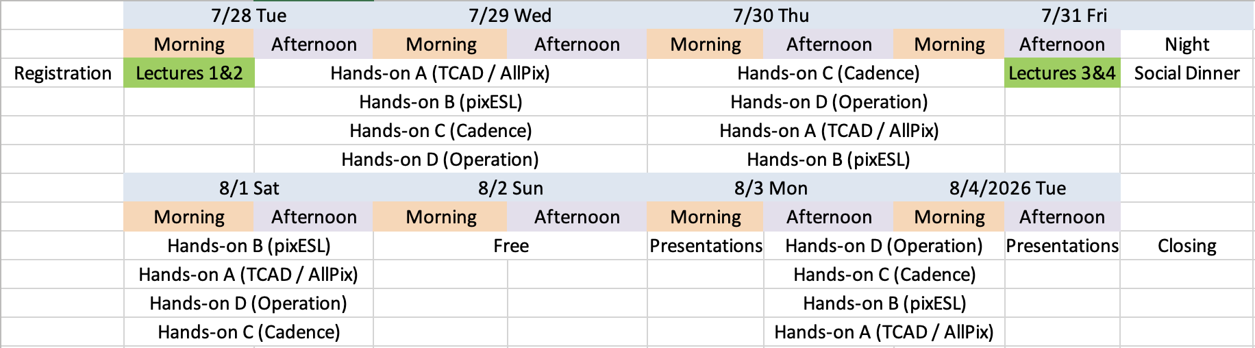
Main target of the academy is hands-on exercises. Participants will proceed through four sets of hands-on exercises and follow four lectures. Students will close their hands-on with a light presentation to highlight their conclusions on the topic.
Hands-on A: Physical sensor simulation with TCAD / Allpix squared.
Simulation of the pixel sensing part of MAPS. Evaluate charge collection efficiency and evolution with charge collection node configuration.
Hands-on B: Analog+Digital part with PixESL.
PixESL applies the Electronics System Level design concept to pixel detectors, offering a virtual environment where both analog and digital components can be modeled, integrated, and analyzed, from particle hits to off-chip data links.
Hands-on C: Microelectronics design for small pixel structure or matrix with Cadence
Simulation of MAPS sensor chip with Cadence. Design of chip structure, readout circiut, power and control part.
Hands-on D: MAPS operation
Operating MALTA2 or MIMOSA28 MAPS sensor. Detailed calibration procedure of MALTA2 or tracking of actual charged particles with RI source (Sr90) and small permanent magnet.
Lectures cover following aspects:
- Introduction to monolithic concept, target performances, and technical aspect to design and produce the MAPS.
- Recent developments towards future experiments in high energy physics and their extended applications.